Theory of Operation#
System Architecture Overview#
The XVF3800 system subdivides into two major sections: a Control Plane and a Data Plane.
The Control Plane includes all control interfaces, related logic, and housekeeping functions. Control Plane functions have low performance requirements, relaxed timing constraints, and complex logic. The XVF3800 design uses a Real Time Operating System (RTOS) to distribute Control Plane functionality across xCORE tile boundaries.
The Data Plane includes all functions that handle audio processing. These functions have hard real-time constraints and operate isochronously. They generally pass their audio data using buffers. The xCORE processor package imposes a constraint on Data Plane functions receiving data from or providing data to an external source due to the number and width of ports connected to physical pins within the package. The XVF3800 operates the Data Plane functions bare-metal, i.e. without the help of an RTOS.
Both the Control Plane and the Data Plane consist of several modules.
Control Plane Modules#
The Control Plane includes the following modules:
Device Control (DC)
Device Firmware Update controller (DFU)
General Purpose Input and Output (GPIO)
Human Interface Device (HID)
Input Output Configuration (IO Config)
Inter-Integrated Circuit Master (I2C Master)
Inter-Integrated Circuit Slave (I2C Slave)
Quad Serial Peripheral Interface (QSPI)
Serial Peripheral Interface Slave (SPI Slave)
Servicers (SER)
Data Plane Modules#
The Data Plane includes the following modules:
Acoustic Echo Cancellation (AEC)
Audio Manager (AM)
Beamforming and Post-processing (BAP)
Customer DSP (DSP)
Inter-IC Sound (I2S)
Microphone Array (MIC)
Software Phase-Locked Loop (SW PLL)
Universal Serial Bus (USB)
Control Plane Module Responsibilities#
Device Control#
The Device Control module handles the transfer of control messages between a host and the device. It connects to the host control interface, e.g. I2C Slave, SPI Slave or USB, on one end and the command servicers on the other end. It routes a command and its response between the host control interface and the intended servicer for that command.
Device Firmware Update Controller#
The Device Firmware Update (DFU) controller processes DFU messages received from a host control interface, e.g. I2C Slave, SPI Slave or USB, and interacts with the QSPI Flash module to read/write to the external flash.
General Purpose Input Output#
The General Purpose Input Output (GPIO) module reads General Purpose Input (GPI) pins and writes to General Purpose Output (GPO) pins. These pins allow device interaction with buttons, sliders or knobs for input and Light Emitting Diodes (LEDs) for output. The GPIO module includes the logic to drive GPO pins using Pulse-Width Modulation (PWM).
Human Interface Device#
The Human Interface Device (HID) module allows the XVF3800 to operate as a human interface device according to the USB Human Interface Devices specification. Compliance with the USB HID specification allows host devices to interact with physical controls and indicators connected to the XVF3800 through the GPIO module such as buttons.
Input Output Configuration#
The Input Output Configuration module configures GPIO devices and an attached Digital to Analogue Converter (DAC). The number of GPIO devices can be extended using the I2C-to-GPIO expander. An example of the IO expander is described in the Expanding available IO for extended HID support section.
Inter-Integrated Circuit Master#
The Inter-Integrated Circuit Master (I2C Master) module provides an XVF3800-clocked I2C data transport for DAC configuration.
Inter-Integrated Circuit Slave#
The Inter-Integrated Circuit Slave (I2C Slave) module provides an externally-clocked I2C data transport for receiving and responding to control commands including the Direction of Arrival command. The XVF3800 cannot include both this module and the Serial Peripheral Interface Slave module in the same build configuration.
Quad Serial Peripheral Interface#
The Quad Serial Peripheral Interface (QSPI) module provides a QSPI data transport for input and output to an attached QSPI Flash memory device. The XVF3800 uses this data transport when booting up from QSPI Flash and during the DFU process.
Serial Peripheral Interface Slave#
The Serial Peripheral Interface (SPI) Slave module provides an externally-clocked SPI data transport for receiving and responding to control commands including the Direction of Arrival command. The XVF3800 cannot include both this module and the Inter-Integrated Circuit Slave module in the same build configuration.
Servicers#
A set of Servicer (SER) modules handle requests from the Device Control module to get or set controllable parameters. It also provides a response back to the Device Control module. Each Servicer handles a request either on its own or through an underlying resource. When using an underlying resource, each Servicer manages the associated control packet queue and ensures thread safety when modifying shared memory or altering a Data Plane module’s controllable parameter.
Data Plane Module Responsibilities#
Acoustic Echo Cancellation#
The Acoustic Echo Cancellation (AEC) module removes from the microphone signal the acoustic echos of the reference signal projected into the room by the loudspeaker.
Audio Manager#
The Audio Manager (AM) performs a number of functions. It collects individual samples from the microphone array and the reference signal source, and it assembles them into a block for further audio processing. It prepares the reference and microphone signals for acoustic processing by, for instance, changing the reference signal sample rate, amplifying either signal as required, converting them between integer and floating point format, and/or adding any necessary delay to synchronise them. It also includes an audio packing facility that allows the XVF3800 to send a selection of six 16 kHz signals which it time-division multiplexes into two 48 kHz I2S or USB channels.
Beamforming and Post-processing#
After the completion of acoustic echo cancellation, the Beamforming and Post-processing (BAP) module further enhances the audio signal through the use of a multi-beam beamformer, de-reverberation, generalised side-lobe cancellation, dynamic echo and noise suppression, automatic gain control, and application of a limiter.
Customer DSP#
The Customer DSP module includes two separate digital signal processing functions set aside to allow customisation of signals as desired for a particular product. The first function allows the customer to alter the reference signal before use by the Acoustic Echo Cancellation module and transmission over I2S. This function operates at the audio interface sample rate. The second function allows the customer to add processing after the signal emerges from the Beamforming and Post-processing module. This function operates at the internal audio processing sample rate. In it, the customer has access to all four beam signals produced by the BAP module and to the residual signals produced by the AEC module.
Inter-IC Sound#
The Inter-IC Sound (I2S) module provides an audio interface to an integrated processor which supplies the reference signal, consumes the processed audio signal, or both. It also includes an audio unpacking facility that allows the XVF3800 to receive the 16 kHz reference signal and four 16 kHz substitute microphone signals as two 48 kHz time-division multiplexed I2S channels.
Microphone Array#
The Microphone Array (MIC) operates four PDM microphones in either a linear or a square/rectangular configuration. It converts the sample rate of the microphone output to match the audio processing sample rate.
Software Phase-Locked Loop#
The Software Phase-Locked Loop (SW PLL) module enables the XVF3800 to synchronize the clock signal used by the microphones with the reference audio signal received via I2S or USB.
Universal Serial Bus#
The Universal Serial Bus (USB) module provides a USB Audio Class 2 (UAC2) interface to a USB host. The host supplies the reference signal, consumes the processed audio signal, or both. This module includes an audio unpacking facility that allows the XVF3800 to receive a 16 kHz reference signal and four 16 kHz substitute microphone signals as two 48 kHz time-division multiplexed USB channels. It also provides a control interface, a DFU interface, and a HID interface used by the Control Plane.
Product Configurations#
The XVF3800 supports two primary use cases:
Integrated device
USB accessory
The integrated device use case embeds the XVF3800 within a system that includes a separate, primary microcontroller. The primary microcontroller provides the reference signal to the XVF3800, receives the processed microphone signal from the XVF3800, and initiates any control commands sent to the XVF3800. It also provides all system functionality outside of the audio processing performed by the XVF3800.
The USB accessory use case embeds the XVF3800 within a system that connects to a USB host. The USB host provides the reference signal, receives the processed microphone signal, initiates any control commands, and provides all functionality outside of the XVF3800.
Interface variations for each use case appear in the table below:
Interface Attribute |
Integrated Device |
USB Accessory |
|---|---|---|
Control Protocol |
I2C slave or SPI slave |
USB |
Data Bit Depth |
32 |
16, 24, or 32 |
Data Protocol |
I2S slave |
USB and I2S master |
Master Clock |
Derived or Input |
Output |
All use cases support either a linear or a square/rectangular geometry of four microphones. Likewise, all use cases support either 16 kHz or 48 kHz operation of the data interface.
A system diagram for each use case appears in Fig. 35 and Fig. 36.
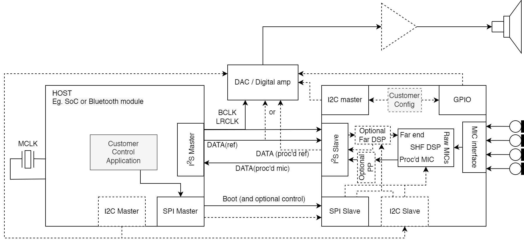
Fig. 35 XVF3800 Integrated Device System Diagram#
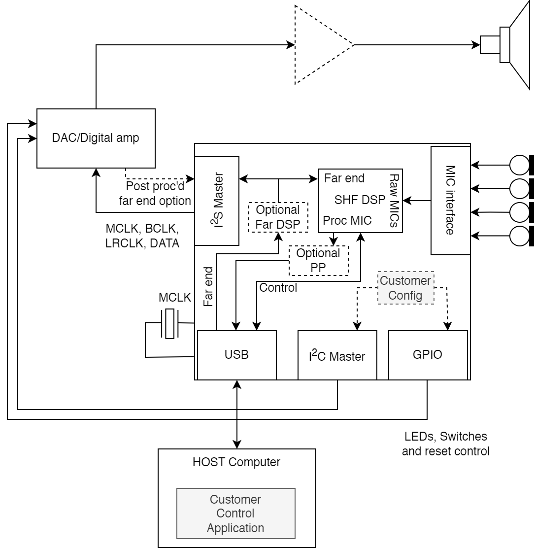
Fig. 36 XVF3800 USB Accessory System Diagram#
Module Placement and Interconnection#
The diagrams in this section show the location of the XVF3800 modules on the two tiles of the xcore.ai and the interconnections between them.
Note
These diagrams do not depict logical cores or channel interconnections.
One diagram is included for the USB Accessory (Fig. 39) use case. The Integrated Device use case supports a control data transport over either SPI or I2C, so two diagrams (Fig. 37 and Fig. 38) appear for it.
Integrated Device with SPI Control#
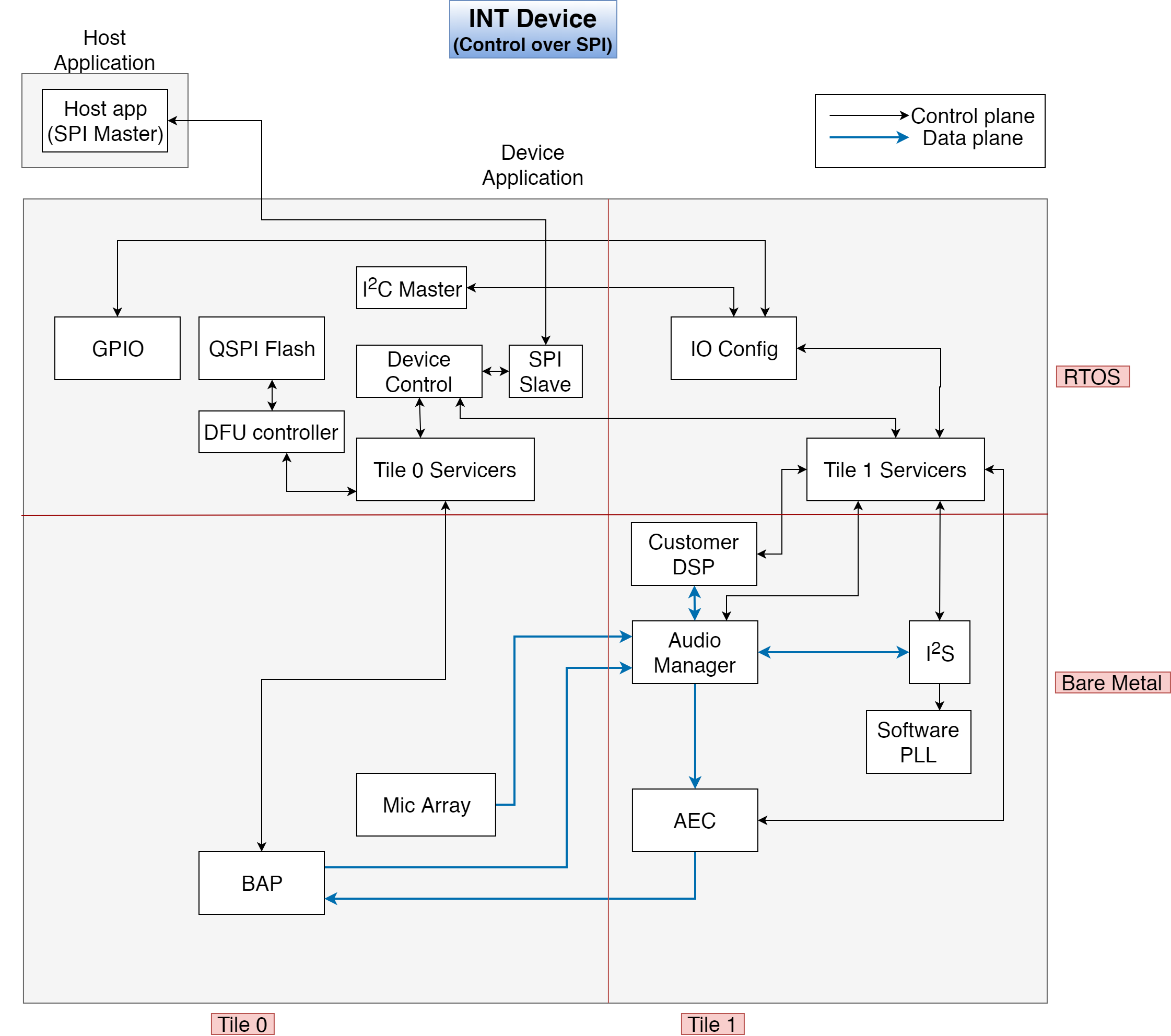
Fig. 37 XVF3800 Integrated Device (SPI control) Location Diagram#
Integrated Device with I2C Control#

Fig. 38 XVF3800 Integrated Device (I2C control) Location Diagram#
USB Accessory#
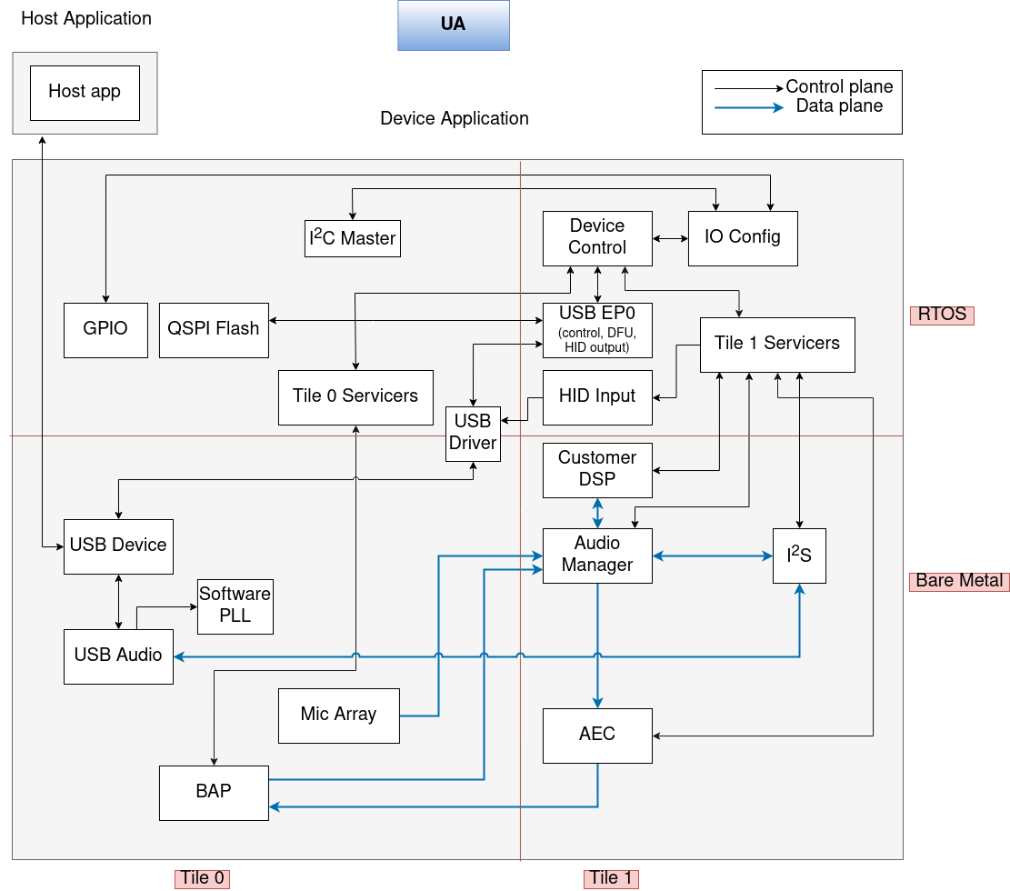
Fig. 39 XVF3800 USB Accessory Location Diagram#
Control Plane Detailed Design#
Control Plane Structure and Operation#
Fig. 40 shows the modules involved in processing control commands. In order to concentrate on their processing, it does not include Control Plane modules, such as the DFU controller, HID, I2C Master or QSPI, that are not directly involved with control command processing.
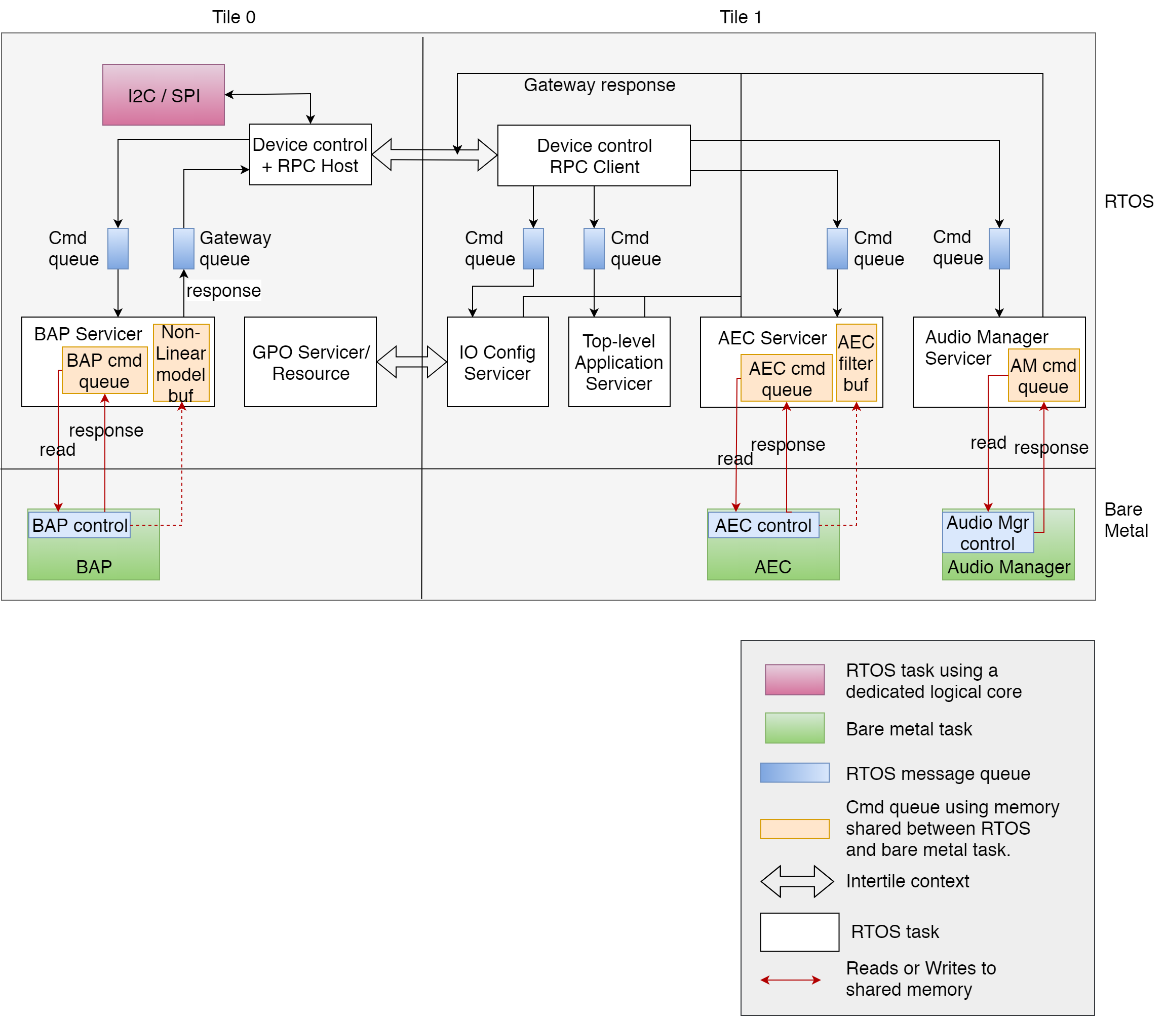
Fig. 40 XVF3800 Control Plane Components Diagram#
Fig. 41 shows the interaction between the Device Control module and a Servicer. In this diagram, boxes with the same colour reside in the same RTOS task.
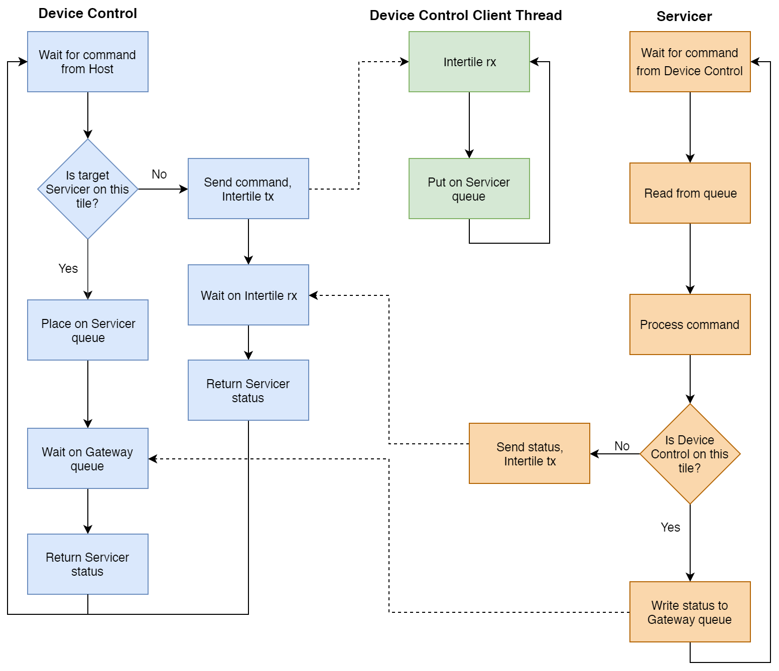
Fig. 41 XVF3800 Device Control – Servicer Flow Chart#
This diagram shows a critical aspect of Control Plane operation. The Device Control module, having placed a command on a Servicer’s command queue, waits on either the Gateway queue or on the Inter-tile context for a response. As a result, it ensures processing of a single control command at a time. Limiting Control Plane operation to a single command in-flight reduces the complexity of the control protocol and eliminates several potential error cases.
Note
Since the Control Plane design requires the host application to poll read commands, limiting operation to a single command in-flight does not limit operation to a single read transaction at a time. For example, a host application may issue a read command to a particular Servicer, receive a status value indicating that it should poll the device for the completion of that read operation, issue a second read command to the same or a different Servicer, receive a status value indicating that it should poll the device for the completion of the second read operation, and then issue additional read commands for either operation in any order until they complete.
Control Protocol#
The XVF3800 uses a packet protocol to receive control commands and send each corresponding response. Because packet transmission occurs over a very short-haul transport, e.g. I2C or SPI, or as the payload within a USB packet, the protocol does not include fields for error detection or correction such as start-of-frame and end-of-frame symbols, a cyclical redundancy check or an error correcting code. Fig. 42 depicts the structure of each packet.
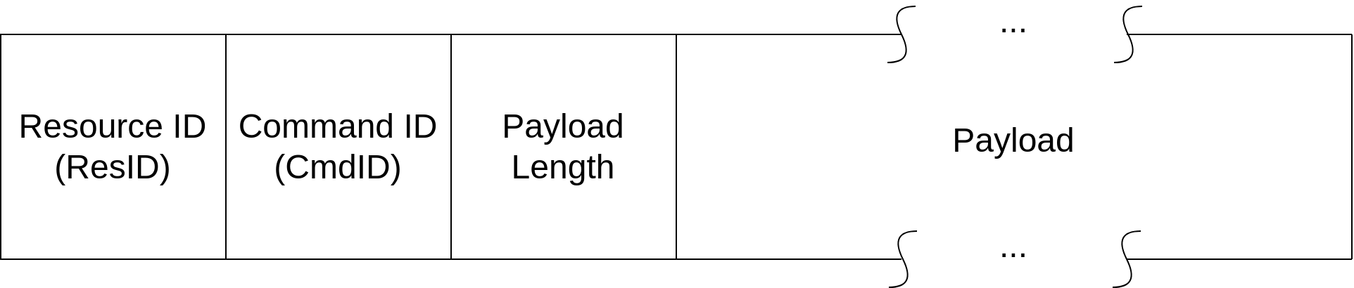
Fig. 42 XVF3800 Control Plane Packet Diagram#
Packets containing a response from the XVF3800 to the host application place a status value in the first byte of the payload.
Data Plane Detailed Design#
Fig. 43 shows the activities within each Data Plane logical core.
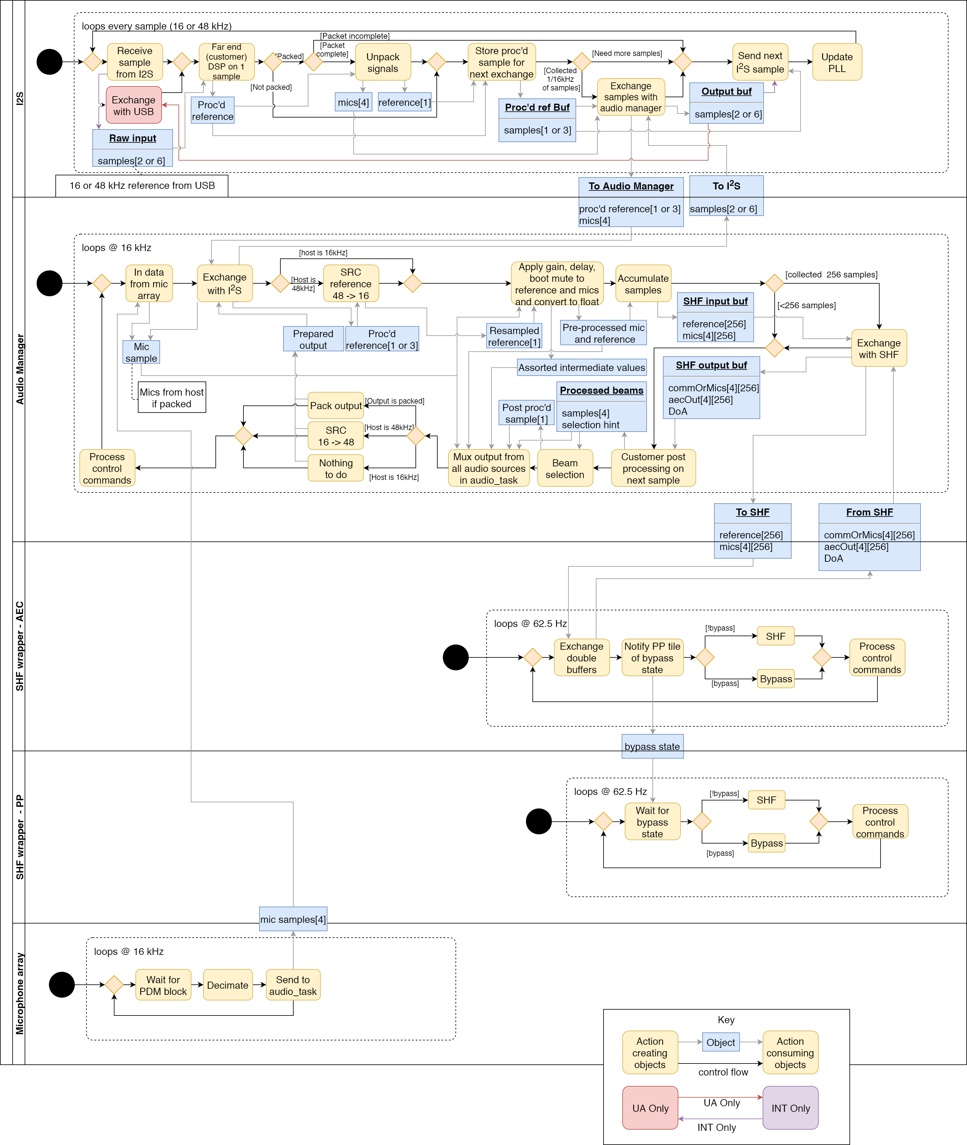
Fig. 43 XVF3800 Data Plane Activity Diagram#
The portion of the Customer DSP module that allows processing of the reference signal prior to use by the Acoustic Echo Cancellation module appears in the I2S logical core. The other portion of the Customer DSP module, which allows further processing of the audio produced by the Beamforming and Post-processing module, appears in the Audio Manager logical core.
The Software Phase Locked Loop module appears in the I2S logical core. The other Data Plane modules each appear in the logical core of the same name.
Device Firmware update (DFU) Design#
The Device Firmware Update (DFU) allows updating the firmware of the device from a host computer, and it can be performed over I2C or USB. This interface closely follows the principles set out in version 1.1 of the Universal Serial Bus Device Class Specification for Device Firmware Upgrade, including implementing the state machine and command structure described there.
The DFU process is internally managed by the DFU controller module within the firmware. This module is tasked with overseeing the DFU state machine and executing DFU operations. The list of states and transactions are represented in the diagram in Fig. 44.
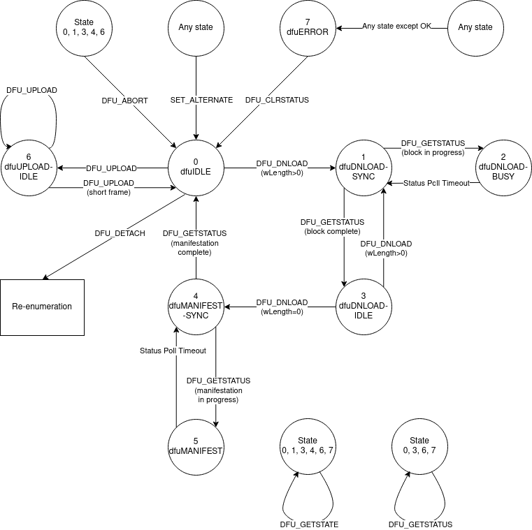
Fig. 44 State diagram of the DFU operations#
The main differences with the state diagram in version 1.1 of Universal Serial Bus Device Class Specification for Device Firmware Upgrade are:
the
appIDLEandappDETACHstates are not implemented, and the device is started in thedfuIDLEstatethe device goes into the
dfuIDLEstate when aSET_ALTERNATEmessage is receivedthe device is rebooted when a
DFU_DETACHcommand is received.
The DFU allows the following operations:
download of an upgrade image to the device
upload of factory and upgrade images from the device
reboot of the device.
The rest of this section describes the message sequence charts of the supported operations.
A message sequence chart of the download operation is below:
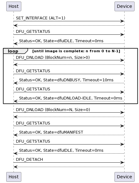
Fig. 45 Message sequence chart of the download operation#
Note
The end of the image transfer is indicated by a DFU_DNLOAD message of size 0.
Note
The DFU_DETACH message is used to trigger the reboot.
Note
For the I2C implementation, specification of the block number in download is not supported; all downloads must start with block number 0 and must be run to completion. The device will track this progress internally.
A message sequence chart of the reboot operation is below:
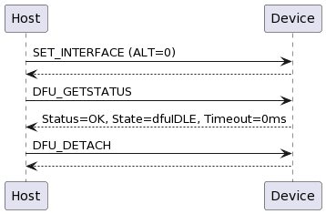
Fig. 46 Message sequence chart of the reboot operation#
Note
The DFU_DETACH message is used to trigger the reboot.
A message sequence chart thisof the upload operation is below:
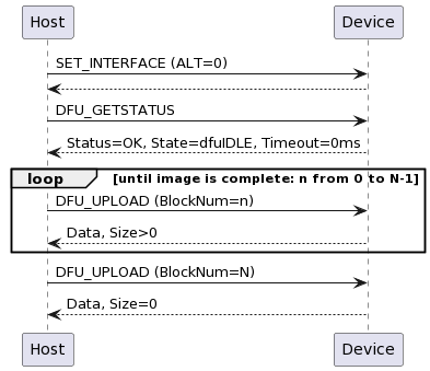
Fig. 47 Message sequence chart of the upload operation#
Note
The end of the image transfer is indicated by a DFU_UPLOAD message of size less than the transport medium maximum; this is 256 bytes in UA and 128 bytes in INT.
DFU over USB implementation#
The UA variant of the device make use of a USB connection for handling DFU operations. This interface is a relatively standard, specification-compliant implementation. The implementation is encapsulated within the tinyUSB library, which provides a USB stack for the XVF3800.
DFU over I2C implementation#
The INT variant of the device presents a DFU interface that may be controlled over I2C.
The INT DFU state machine is driven by use of control commands, as described in Control Plane Detailed Design. The DFU state machine has its own servicer, which then interacts with a separate RTOS task in order to asynchronously perform flash read/write operations.
Mirroring the USB DFU specification, the INT implementation supports a set of 9 control commands intended to drive the state machine, along with an additional 2 utility commands:
Name |
ID |
Length |
Payload Structure |
Purpose |
|---|---|---|---|---|
DFU_DETACH |
0 |
1 |
Payload unused |
Write-only command. Restarts the device. Payload is required for protocol, but is discarded within the device. This command has a defined purpose in the USB DFU specification, but in a deviation to that specification it is used with I2C simply to reboot the device. Future versions of the XMOS DFU-by-device-control protocol (but not future versions of this product) may choose to alter the function of this command to more closely align with the USB DFU specification. |
DFU_DNLOAD |
1 |
130 |
2 bytes length marker, followed by 128 bytes of data buffer |
Write-only command. The first two bytes indicate how many bytes of data are being transmitted in this packet. These bytes are little-endian, so byte 0 represents the low byte and byte 1 represents the high byte of an unsigned 16b integer. The remaining 128 bytes are a data buffer for transfer to the device. All control command packets are a fixed length, and therefore all 128 bytes must be included in the command, even if unused. For example, a payload with length of 100 should have the first 100 bytes of data set, but must send an additional 28 bytes of arbitrary data. |
DFU_UPLOAD |
2 |
130 |
2 bytes length marker, followed by 128 bytes of data buffer |
Read-only command. The first two bytes indicate how many bytes of data are being transmitted in this packet. These bytes are little-endian, so byte 0 represents the low byte and byte 1 represents the high byte of an unsigned 16b integer. The remaining 128 bytes are a data buffer of data received from the device. All control command packets are a fixed length, and therefore this buffer will be padded to length 128 by the device before transmission. The device will, as per the USB DFU specification, mark the end of the upload process by sending a “short frame” - a packet with a length marker less than 128 bytes. |
DFU_GETSTATUS |
3 |
5 |
1 byte representing device status, 3 bytes representing the requested timeout, 1 byte representing the next device state. |
Read-only command. The first byte returns the device status code, as described in the USB DFU specification in the table in section 6.1.2. The next 3 bytes represent the amount of time the host should wait, in ms, before issuing any other commands. This timeout is used in the DNLOAD process to allow the device time to write to flash. This value is little-endian, so bytes 1, 2, and 3 represent the low, middle, and high bytes respectively of an unsigned 24b integer. The final byte returns the number of the state that the device will move into immediately following the return of this request, as described in the USB DFU specification in the table in section 6.1.2. |
DFU_CLRSTATUS |
4 |
1 |
Payload unused |
Write-only command. Moves the device out of state 10, dfuERROR. Payload is required for protocol, but is discarded within the device. |
DFU_GETSTATE |
5 |
1 |
1 byte representing current device state. |
Read-only command. The first (and only) byte represents the number of the state that the device is currently in, as described in the USB DFU specification in the table in section 6.1.2. |
DFU_ABORT |
6 |
1 |
Payload unused |
Write-only command. Aborts an ongoing upload or download process. Payload is required for protocol, but is discarded within the device. |
DFU_SETALTERNATE |
64 |
1 |
1 byte representing either factory (0) or upgrade (1) DFU target images |
Write-only command. Sets which of the factory or upgrade images should be targeted by any subsequent upload or download commands. Use of this command entirely resets the DFU state machine to initial conditions: the device will move to dfuIDLE, clear all error conditions, wipe all internal DFU data buffers, and reset all other DFU state apart from the DFU_TRANSFERBLOCK value. This command is included to emulate the SET_ALTERNATE request available in USB. |
DFU_TRANSFERBLOCK |
65 |
2 |
2 bytes, representing the target transfer block for an upload process. |
Read/write command. Sets/gets a 2 byte value specifying the transfer block number to use for a subsequent upload operation. A complete image may be conceptually divided into 128-byte blocks. These blocks may then be numbered from 0 upwards. Setting this value sets which block will be returned by a subsequent DFU_UPLOAD request. This value is initialised to 0, and autoincrements after each successful DFU_UPLOAD request has been serviced. Therefore, to read a whole image from the start, there is no need to issue this command - this command need only be used to select a specific section to read. Because this value is automatically incremented after a DFU_UPLOAD command is successfully serviced, reading it will give the value of the next block to be read (and this will be one greater than the previous block read, if it has not been altered in the interim). This value is reset to 0 at the successful completion of a DFU_UPLOAD process. It is not reset after a DFU_ABORT, nor after a DFU_SETALTERNATE call. This command is included to emulate the ability in a USB request to send values in the header of the request - the device control protocol used here does not allow sending any data with a read request such as DFU_UPLOAD. |
DFU_GETVERSION |
88 |
3 |
3 bytes, representing major.minor.patch version of device |
Read-only command. Bytes 0, 1, and 2 represent the major, minor, and patch versions respectively of the device. This is a utility command intended to provide an easy mechanism by which to verify that a firmware download has been successful. |
DFU_REBOOT |
89 |
1 |
Payload unused |
Write-only command. Restarts the device. Payload is required for protocol, but is discarded within the device. This is a utility command intended to provide a clear and unambiguous interface for restarting the device. Use of this command should be preferred over DFU_DETACH for this purpose. |
These commands are then used to drive the state machine described in the Device Firmware update (DFU) Design.
When writing a custom compliant host application, the use of XMOS’ fwk_rtos library is advised; the device_control library provided there gives a host API that can communicate effectively with the XVF3800, as demonstrated in the xvf_host application. However, a description of the I2C bus activity during the execution of the above DFU commands is provided below, in the instance that usage of the device_control library is inconvenient or impossible.
The XVF3800’s I2C address is set by default as 0x2C. This may be
confirmed by examination of the I2C_ADDRESS field in the
transport_config.yaml file, found in the release package at
sources/app_xvf3800/autogeneration/yaml_files/settings_and_defaults.
The XVF3800’s I2C address may also be altered by editing this file.
The DFU resource has an internal “resource ID” of 0xF0. This maps to the
register that read/write operations on the DFU resource should target -
therefore, the register to write to will always be 0xF0.
To issue a write command (e.g. DFU_SETALTERNATE):
First, set up a write to the device address. For a default device configuration, a write operation will always start by a write token to 0x2C (START, 7 bits of address [0x2C], R/W bit [0 to specify write]), wait for ACK, followed by specifying the register to write [Resource ID 0xF0] (and again wait for ACK).
Then, write the command ID (in this example, 64 [0x40]) from the above table.
Then, write the total transfer size, including the register byte. In this example, that will be 4 bytes (register byte, command ID, length byte, and 1 byte of payload), so write 0x04.
Finally, send the payload - e.g. 1 to set the alternate setting to “upgrade”.
The full sequence for this write command will therefore be START, 7 bits of address [0x2C], 0 (to specify write), hold for ACK, 0xF0, hold for ACK, 0x40, hold for ACK, 0x04, hold for ACK, 0x01, hold for ACK, STOP.
To complete the transaction, the device must then be queried; set up a read to 0x2C (START, 7 bits of address [0x2C], R/W bit [1 to specify read], wait for ACK). The device will clock-stretch until it is ready, at which point it will release the clock and transmit one byte of status information. This will be a value from the enum
control_ret_tfromdevice_control_shared.h, found insources\modules\fwk_xvf\modules\rtos\modules\sw_services\device_control\api.
To issue a read command (e.g. DFU_GETSTATUS):
Set up a write to the device; as above, this will mean sending START, 7 bits of device address [0x2C], 0 (to specify write), hold for ACK. Send the DFU resource ID [0xF0], hold for ACK.
Then, write the command ID (in this example, 3), bitwise ANDed with 0x80 (to specify this as a read command) - in this example therefore 0x83 should be sent, and hold for ACK.
Then, write the total length of the expected reply. In this example, the command has a payload of 5 bytes. The device will also prepend the payload with a status byte. Therefore, the expected reply length will be 6 bytes [0x06]. Hold for ACK.
Then, issue a repeated START. Follow this with a read from the device: the repeated START, 7 bits of device address [0x2C], 1 (to specify read), hold for ACK. The device will clock-stretch until it is ready. It will then send a status byte (from the enum
control_ret_tas described above), followed by a payload of requested data - in this example, the device will send 5 bytes. ACK each received byte. After the last expected byte, issue a STOP.
It is heavily advised that those wishing to write a custom host application to drive the DFU process for the XVF3800 over I2C familiarise themselves with version 1.1 of the Universal Serial Bus Device Class Specification for Device Firmware Upgrade.
HID Interface design#
The UA variant of the device presents a USB HID interface. The HID interface adds support for USB standard input and output reports for a telephony device.
HID descriptors#
As shown in the trace captured during device enumeration (Fig. 48), the HID interface presents itself as interface 5 in the configuration descriptor. The device enumerates with Endpoint 2 as the HID Input endpoint which is responsible for sending HID input reports to the host.
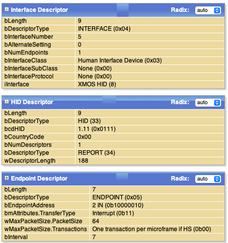
Fig. 48 HID descriptor during enumeration#
The device also supports using the UC Qualification (UCQ) descriptor for HID to inform the host of its capabilities. The UCQ string descriptor returned by the device is “UCQ01001000001000” indicating a speakerphone device with AEC capability.
Input reports are sent in response to button presses on the device or in response to specific HID output reports. HID output reports are sent by the host on Endpoint 0. Feature reports are sent and received by the host on Endpoint 0.
Note
While the HID device descriptor currently describes one feature report, the current HID implementation doesn’t support parsing feature reports received from the host or responding with a non-zero feature report to the host.
The HID descriptor structure is transcluded below from sources/modules/fwk_xvf/modules/xvf/src/usb/config/usb_descriptors.c:
uint8_t const desc_hid_report[] =
{
  TUD_HID_REPORT_DESC_MISC_BUTTONS   (HID_REPORT_ID(REPORT_ID_MISC_BUTTONS            )),
  TUD_HID_REPORT_DESC_VOLUME_BUTTONS (HID_REPORT_ID(REPORT_ID_VOLUME_BUTTONS            )),
  TUD_HID_REPORT_DESC_TEAMS_ASP      ( HID_REPORT_ID(REPORT_ID_TEAMS_ASP              )),
  TUD_HID_REPORT_DESC_TEAMS_BUTTON   ( HID_REPORT_ID(REPORT_ID_TEAMS_BUTTON           )),
};
The macros defining the individual reports that are part of the desc_hid_report structure are transcluded below from
sources/modules/fwk_xvf/modules/xvf/src/usb/config/hid_telephony_device.h:
#define TUD_HID_REPORT_DESC_MISC_BUTTONS(...) \
  HID_USAGE_PAGE ( HID_USAGE_PAGE_TELEPHONY                  ) ,\
  HID_USAGE      ( HID_USAGE_TELEPHONY_PHONE                 ) ,\
  HID_COLLECTION ( HID_COLLECTION_APPLICATION                ) ,\
    /* Report ID if any */\
    __VA_ARGS__ \
    HID_USAGE       ( HID_USAGE_TELEPHONY_HOOKSWITCH         ) ,\
    HID_LOGICAL_MIN ( 0                                      ) ,\
    HID_LOGICAL_MAX ( 1                                      ) ,\
    HID_REPORT_COUNT( 1                                      ) ,\
    HID_REPORT_SIZE ( 1                                      ) ,\
    HID_INPUT       ( HID_DATA | HID_VARIABLE | HID_ABSOLUTE ) ,\
    HID_USAGE       ( HID_USAGE_TELEPHONY_PHONE_MUTE         ) ,\
    HID_INPUT       ( HID_DATA | HID_VARIABLE | HID_ABSOLUTE ) ,\
    HID_USAGE       ( HID_USAGE_TELEPHONY_FLASH              ) ,\
    HID_INPUT       ( HID_DATA | HID_VARIABLE | HID_ABSOLUTE ) ,\
    HID_USAGE       ( HID_USAGE_TELEPHONY_REDIAL             ) ,\
    HID_INPUT       ( HID_DATA | HID_VARIABLE | HID_ABSOLUTE ) ,\
    HID_USAGE_PAGE  ( HID_USAGE_PAGE_BUTTON                  ) ,\
    /* This button has been chosen to support the HOLD procedure in Teams */ \
    HID_USAGE       ( HID_USAGE_BUTTON_7                     ) ,\
    HID_INPUT       ( HID_DATA | HID_VARIABLE | HID_ABSOLUTE ) ,\
    /* 3 bit padding */ \
    HID_REPORT_COUNT( 1                                      ) ,\
    HID_REPORT_SIZE ( 3                                      ) ,\
    HID_INPUT       ( HID_CONSTANT                           ) ,\
    HID_USAGE_PAGE  ( HID_USAGE_PAGE_TELEPHONY               ) ,\
    HID_USAGE       ( HID_USAGE_TELEPHONY_KEYPAD             ) ,\
    HID_LOGICAL_MIN ( 1                                      ) ,\
    HID_LOGICAL_MAX ( 12                                     ) ,\
    HID_REPORT_COUNT( 1                                      ) ,\
    HID_REPORT_SIZE ( 4                                      ) ,\
    HID_USAGE_MIN   ( 0xB0                                   ) ,\
    HID_USAGE_MAX   ( 0xBB                                   ) ,\
    HID_INPUT       ( HID_DATA | HID_ARRAY | HID_ABSOLUTE    ) ,\
    HID_LOGICAL_MIN ( 0                                      ) ,\
    HID_LOGICAL_MAX ( 1                                      ) ,\
    /* 4 bit padding */ \
    HID_REPORT_COUNT( 1                                      ) ,\
    HID_REPORT_SIZE ( 4                                      ) ,\
    HID_INPUT       ( HID_CONSTANT                           ) ,\
    HID_USAGE_PAGE  ( HID_USAGE_PAGE_LED                     ) ,\
    HID_USAGE       ( HID_USAGE_LED_OFF_HOOK                 ) ,\
    HID_LOGICAL_MIN ( 0                                      ) ,\
    HID_LOGICAL_MAX ( 1                                      ) ,\
    HID_REPORT_COUNT( 1                                      ) ,\
    HID_REPORT_SIZE ( 1                                      ) ,\
    HID_OUTPUT      ( HID_DATA | HID_VARIABLE | HID_ABSOLUTE ) ,\
    HID_USAGE       ( HID_USAGE_LED_MUTE                     ) ,\
    HID_OUTPUT      ( HID_DATA | HID_VARIABLE | HID_ABSOLUTE ) ,\
    HID_USAGE       ( HID_USAGE_LED_RING                     ) ,\
    HID_OUTPUT      ( HID_DATA | HID_VARIABLE | HID_ABSOLUTE ) ,\
    HID_USAGE       ( HID_USAGE_LED_HOLD                     ) ,\
    HID_OUTPUT      ( HID_DATA | HID_VARIABLE | HID_ABSOLUTE ) ,\
    /* 4 bit padding */ \
    HID_REPORT_COUNT( 1                                      ) ,\
    HID_REPORT_SIZE ( 4                                      ) ,\
    HID_OUTPUT      ( HID_CONSTANT                           ) ,\
  HID_COLLECTION_END  \
#define TUD_HID_REPORT_DESC_VOLUME_BUTTONS(...) \
  HID_USAGE_PAGE ( HID_USAGE_PAGE_CONSUMER                   ), \
  HID_USAGE      ( HID_USAGE_CONSUMER_CONTROL                ) ,\
  HID_COLLECTION ( HID_COLLECTION_APPLICATION                ) ,\
    /* Report ID if any */                                      \
    __VA_ARGS__                                                 \
    HID_LOGICAL_MIN ( 0                                      ) ,\
    HID_LOGICAL_MAX ( 1                                      ) ,\
    HID_REPORT_COUNT( 1                                      ) ,\
    HID_REPORT_SIZE ( 1                                      ) ,\
    HID_USAGE       ( HID_USAGE_CONSUMER_VOLUME_INCREMENT   )  ,\
    HID_INPUT       ( HID_DATA | HID_VARIABLE | HID_ABSOLUTE ) ,\
    HID_USAGE       ( HID_USAGE_CONSUMER_VOLUME_DECREMENT    ) ,\
    HID_INPUT       ( HID_DATA | HID_VARIABLE | HID_ABSOLUTE ) ,\
    /* 6 bit padding */                                         \
    HID_REPORT_COUNT( 1                                      ) ,\
    HID_REPORT_SIZE ( 6                                      ) ,\
    HID_INPUT       ( HID_CONSTANT                           ) ,\
  HID_COLLECTION_END  \
#define TUD_HID_REPORT_DESC_TEAMS_BUTTON(...) \
  HID_USAGE_PAGE_N ( 0xFF99, 2                               ) ,\
  HID_USAGE      ( 0x01                                      ) ,\
  HID_COLLECTION ( HID_COLLECTION_APPLICATION                ) ,\
    /* Report ID if any */                                      \
    __VA_ARGS__                                                 \
    HID_LOGICAL_MIN ( 0                                      ) ,\
    HID_LOGICAL_MAX ( 1                                      ) ,\
    HID_REPORT_COUNT( 1                                      ) ,\
    HID_REPORT_SIZE ( 1                                      ) ,\
    HID_USAGE       ( 0x04                                   ) ,\
    HID_INPUT       ( HID_DATA | HID_VARIABLE | HID_RELATIVE ) ,\
    /* 7 bit padding */                                         \
    HID_REPORT_COUNT( 1                                      ) ,\
    HID_REPORT_SIZE ( 7                                      ) ,\
    HID_INPUT       ( HID_CONSTANT                           ) ,\
  HID_COLLECTION_END                                            \
#define TUD_HID_REPORT_DESC_TEAMS_ASP(...) \
  HID_USAGE_PAGE_N ( 0xFF99, 2                              ) ,\
  HID_USAGE        ( 0x03                                   ) ,\
  HID_COLLECTION   ( HID_COLLECTION_APPLICATION             ) ,\
    /* Report ID if any */                                     \
    __VA_ARGS__                                                \
    HID_LOGICAL_MIN   ( 0                                   ) ,\
    HID_LOGICAL_MAX_N ( 255, 2                              ) ,\
    HID_USAGE_MIN     ( 0x00                                ) ,\
    HID_USAGE_MAX     ( 0xff                                ) ,\
    HID_REPORT_COUNT_N( 63, 2                               ) ,\
    HID_REPORT_SIZE   ( 8                                   ) ,\
    HID_FEATURE       ( HID_DATA | HID_VARIABLE | HID_ABSOLUTE ) ,\
  HID_COLLECTION_END  \
The HID report descriptor translates to three input reports, one output report and one feature report.
Input report ID 1 contains the Hook Switch, Mute, Flash, Redial and the Dialpad buttons.
Note
The current HID implementation doesn’t support Dialpad buttons.
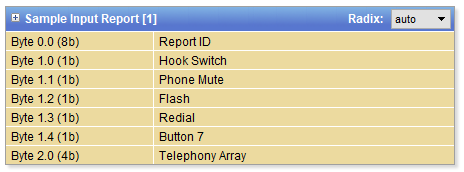
Fig. 49 Input report ID 1#
Output report ID 1 contains the Off-hook, Mute, Ring and Hold LEDs.
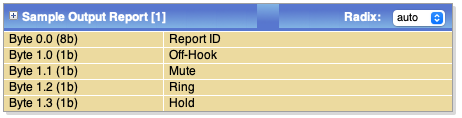
Fig. 50 Output report ID 1#
Input report ID 2 contains the Volume Increment and Volume Decrement buttons.
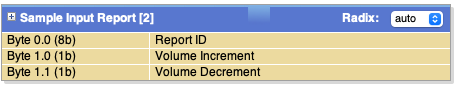
Fig. 51 Input report ID 2#
Input report ID 155 contains a custom button meant to be used as the Teams button.
Note
The Teams button implementation requires the device to respond to feature reports and is currently unimplemented.
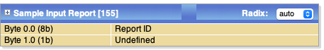
Fig. 52 Input report ID 155#
HID System Design#
The HID interface is implemented in the RTOS. Fig. 53 shows the tasks involved in the HID implementation.
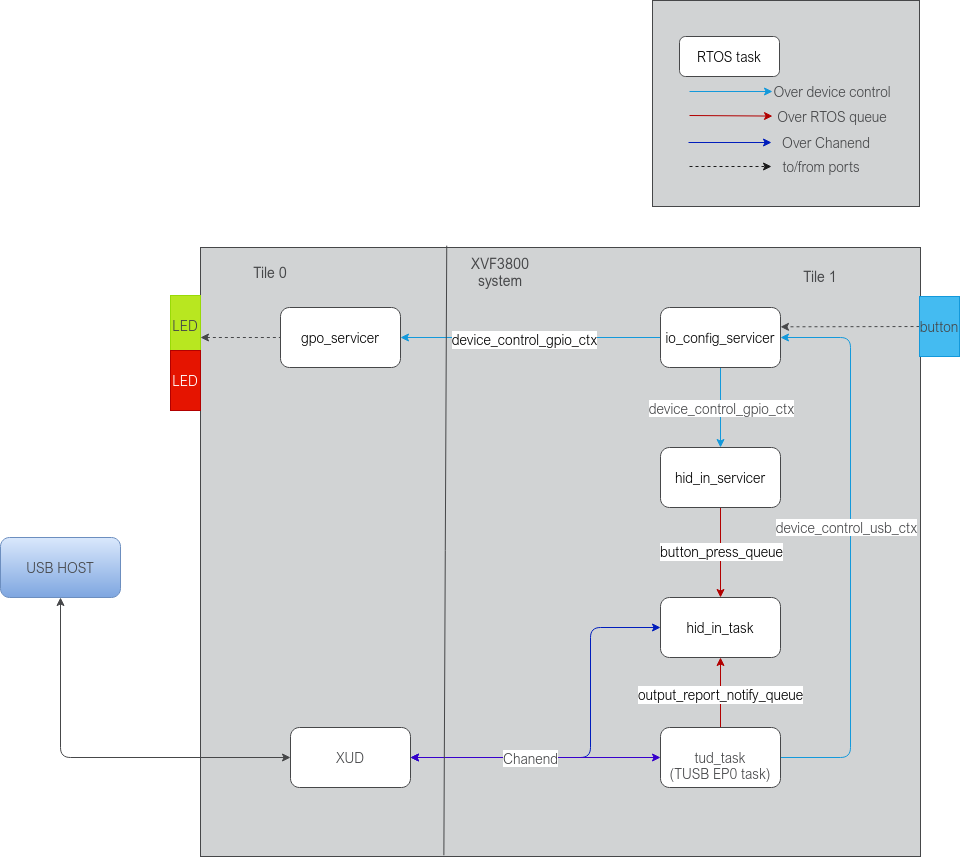
Fig. 53 HID task diagram#
The io_config_servicer detects button presses and notifies a button press event to the hid_in_servicer through a control command sent on the device_control_gpio_ctx. It also forwards the GPO commands for LED control to the gpo_servicer.
The gpo_servicer receives GPO LED commands over the device_control_gpio_ctx and programmes the LEDs.
The hid_in_servicer notifies the hid_in_task of the button press event notifications that it receives from the io_config_servicer.
The tud_task implements USB Endpoint 0 and calls the callback function tud_hid_set_report_cb on receiving a HID output report from the host on Endpoint 0.
If an LED state needs to change in response to the output report, tud_hid_set_report_cb initiates it by sending GPO LED control commands to the io_config_servicer.
tud_hid_set_report_cb also notifies the the hid_in_task when specific output reports are received.
The hid_in_task implements the HID Input endpoint. It is a timer based task that wakes up periodically and sends a HID input report to the host over the HID Input endpoint.
The logic for deciding which report to send is as follows:
If the previous iteration attempted to send a report but could not, re-attempt sending the report,
else, if a One Shot Control (OSC) button press sequence is in progress, send the report to complete the button press sequence,
else, check if there is an output report notification from
tud_hid_set_report_cbthat requires sending an input report in response,else, check if there is a button press notification from
io_config_servicerand send an input report corresponding to the pressed button.
To summarise, Fig. 54 shows the path through which a GPI button press translates into a HID input report, and Fig. 55 shows the path through which a HID output report that the device receives translates to a GPO LED program. Additionally, Fig. 55 also shows the path through which a HID output report translates to a HID input report sent from the device to USB.
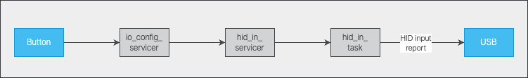
Fig. 54 HID button path#
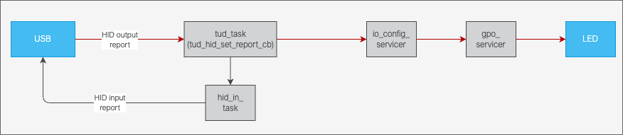
Fig. 55 HID LED path#
HID Initialisation#
During device initialisation, the hid_init function is called to do all HID related initialisations.
The HID button and LED configurations are captured in the hid_button_config_t and hid_led_config_t structures.
These structures contain the mapping from a given HID button to the GPI button on the device and from a given HID LED to
the GPO LED on the device.
The init_hid_button_config function initialises the HID buttons. There is one button on the XK-VOICE-SQ66 development kit (XS1_PORT_4A pin 3) and it’s currently
mapped to the HID Mute button as can be seen in the code transcluded from the init_hid_button_config in sources/modules/fwk_xvf/modules/xvf/src/usb/control_plane/hid_init.c:
    hid_button_config_t config = {.report_id = REPORT_ID_MISC_BUTTONS, .offset = BUTTON_MUTE_OFFSET, .size = 1, .gpi_source = GPI_SOURCE_EVK, .gpi_pin_index = EVK_BUTTON_INDEX, .button_type = BUTTON_TYPE_OSC, .button_press_precondition=HOOKSWITCH_BUTTON};
    hid_button_config[MUTE_BUTTON] = config;
Note the .gpi_source = GPI_SOURCE_EVK and .gpi_pin_index = EVK_BUTTON_INDEX in the code above that map the button on the XK-VOICE-SQ66 development kit to the HID Mute button.
Note
The HID implementation supports two types of buttons, One Shot Control (OSC) and Re-Trigger Control (RTC). The Volume Increment and Volume Decrement buttons are set as RTC while all the other buttons are configured to be of OSC type. For the OSC buttons, only after the button is released, the device sends an input report with the button set to 1 followed by another input report with the button set to 0. For the RTC buttons, in a button press event, an input report with button set to 1 is sent and in a button release event, an input report with button set to 0 is sent by the device.
The init_hid_led_config function initialises the HID LEDs. The Red LED (XS1_PORT_8C, pin 6) on the XK-VOICE-SQ66 development kit is mapped to the MUTE_LED and the Green LED (XS1_PORT_8C, pin 7) on the XK-VOICE-SQ66 development kit
is mapped to the OFFHOOK_LED as shown in the code transcluded from sources/modules/fwk_xvf/modules/xvf/src/usb/control_plane/hid_init.c below:
    hid_led_config_t config = {.report_id = REPORT_ID_MISC_BUTTONS, .offset = LED_OFFHOOK_OFFSET, .gpo_source = GPO_SOURCE_EVK, .gpo_pin_index = EVK_LED_GREEN, .notify_hid_task = true, .trigger_hid_input_index = HOOKSWITCH_BUTTON, .led_mode=LED_MODE_STEADY};
    hid_led_config[OFFHOOK_LED] = config;
Note the .gpo_source = GPO_SOURCE_EVK and .gpo_pin_index = EVK_LED_GREEN in the code above that map the green LED on the XK-VOICE-SQ66 development kit to the HID OffHook LED.
    hid_led_config_t config = {.report_id = REPORT_ID_MISC_BUTTONS, .offset = LED_MUTE_OFFSET, .gpo_source = GPO_SOURCE_EVK, .gpo_pin_index = EVK_LED_RED, .notify_hid_task = false, .trigger_hid_input_index = NO_HID_IN_TRIGGER, .led_mode=LED_MODE_STEADY};
    hid_led_config[MUTE_LED] = config;
Note the .gpo_source = GPO_SOURCE_EVK and .gpo_pin_index = EVK_LED_RED in the code above that map the red LED on the XK-VOICE-SQ66 development kit to the HID Mute LED.
The HID buttons/LEDs to GPIO button/LEDs mapping can be changed by modifying the init_hid_button_config and init_hid_led_config functions.
Modifying the HID to GPIO mapping describes this in detail.
HID Operation#
With the HID Buttons and LEDs initialised as described in HID Initialisation, the following use cases are implemented.
Mute/Unmute device#
When the device is used in an ongoing Teams call, the user pressing the Mute button on the device ends up with the microphone mute status toggled on the Teams client. Fig. 56 depicts this use case. The Mute button is a One Shot Control button type which means that a 0 -> 1 in the button state in the HID report triggers an event and a 1 -> 0 transition in the button state has to happen before the next event. As a result, the Mute button pressed on the device has the device sending two hid reports, with the Mute button set to 1 and 0 respectively.
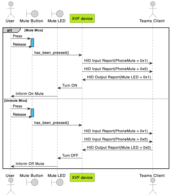
Fig. 56 Mic mute/unmute#
Inform call start#
At the start of the Teams call, the Teams client sends a HID output report with Off-Hook LED set to 1. The device responds with an input report with HookSwitch set to 1. Note that this is an example of the device sending an input report in response to a given HID output report.
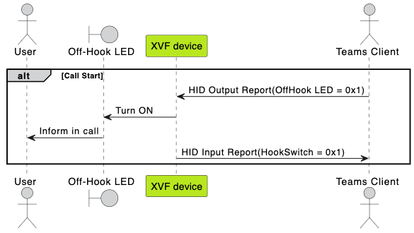
Fig. 57 Call Start#
Inform call end#
Similar to Inform call start, to inform call end, the host sends an output report with Off-Hook set to 0 which the device follows up with an input report with HookSwitch set to 0.
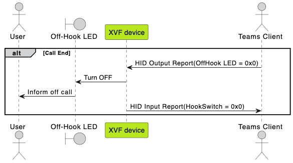
Fig. 58 Call End#
Expanding available IO for extended HID support#
This section describes extending the HID support by expanding the number of GPIOs available on the device for mapping to HID events.
This is done by attaching an IO expander to the XK-VOICE-SQ66 development kit device. IO Expander ICs provide programmable GPIO and are controlled via an interface.
The XVF3800 supports a build configuration (application_xvf3800_ua-io48-lin-io-exp) that adds support for an IO expander connected to the XK-VOICE-SQ66 development kit. The IO expander
used is the PCAL6416A, which is a GPIO expander providing remote IO support and is controlled over the I2C bus.
The PCAL6416A I2C expander (referred to as just I2C expander in the rest of the document) has the I2C slave address of 0x21. Pins 0, 1, 2 and 3 on Port 0 are configured as input pins and are used for extra buttons. The incoming logic levels of these pins is read from the Input port register (00h) of the I2C expander.
The default GPI pin to HID button mapping for the application_xvf3800_ua-io48-lin-io-exp build is summarised in GPI to HID button mapping:
GPI button |
HID button |
|---|---|
I2C expander, register 00h, pin 0 |
Mute button |
I2C expander, register 00h, pin 1 |
Volume Increment button |
I2C expander, register 00h, pin 2 |
Flash button |
I2C expander, register 00h, pin 3 |
Volume Decrement button |
XK-VOICE-SQ66 development kit button, |
HookSwitch button |
This mapping can be seen in the code wihin the #if (IO_EXPANDER_ENABLED) define in the init_hid_button_config function in sources/modules/fwk_xvf/modules/xvf/src/usb/control_plane/hid_init.c.
Pin 4 on Port 0 is configured as an output pin and is used for one extra LED. The output logic level of this pin is written to the Output port register register 02h of the I2C expander.
In addition to the PCAL6416A I2C expander, the I2C expander board that is connected to the XK-VOICE-SQ66 development kit in the application_xvf3800_ua-io48-lin-io-exp build
configuration has another LED, IS31FL3193, that is programmable via the I2C interface on address 0x68.
The default GPO pin to HID LED mapping for the application_xvf3800_ua-io48-lin-io-exp build is summarised in GPO to HID LED mapping:
GPO LED |
HID LED |
|---|---|
PCAL6416A I2C expander, register 02h, pin 4 |
Mute LED |
IS31FL3193 LED |
Ring LED |
IS31FL3193 LED |
Hold LED |
XK-VOICE-SQ66 development kit Green LED, |
Off-Hook LED |
This mapping can be seen in the code within the #if (IO_EXPANDER_ENABLED) define in the init_hid_led_config function in sources/modules/fwk_xvf/modules/xvf/src/usb/control_plane/hid_init.c.
Note
The Ring and Hold LED are mapped to the same GPO LED but with different flash modes (look at the led_mode field initialisation in init_hid_led_config). This allows distinguishing between the two events. The Ring event causes
a fast flash while the Hold event causes a slow flash of the LED. The led_mode field initialisation in the init_hid_led_config configures the flash mode.
System Design#
The system design in HID System Design is extended to add the I2C expander tasks. Fig. 59 describes the extended design:
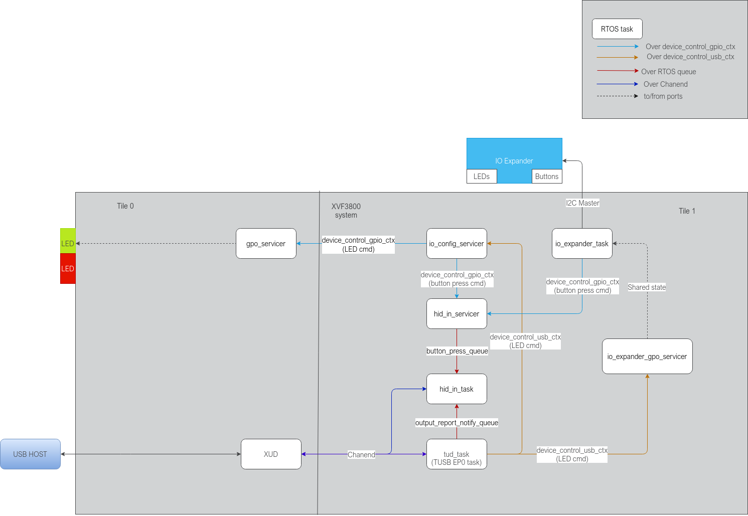
Fig. 59 HID with IO expander task diagram#
The io_expander_task reads button states and programs LEDs on the I2C expander over the I2C master interface.
It is a timer driven task that wakes up periodically, reads the button statuses and notifies button press events to the hid_in_servicer through control commands
sent over the device_control_gpio_ctx. It also configures the I2C expander LEDs if notified to do so by the io_expander_gpo_servicer task.
The io_expander_gpo_servicer handles GPO commands sent from tud_hid_set_report_cb to program LEDs in response to HID output reports. It updates the LED state in a structure shared in memory
with the io_expander_task which then configures the LED registers over the I2C interface.
The hid_in_task gets notified by both io_expander_task and io_config_servicer tasks with different commands sent over the same device control context about button press events.
The tud_hid_set_report_cb sends GPO control commands to io_config_servicer and io_expander_gpo_servicer depending on where the LED that needs to be configured resides.
Fig. 60 shows the updated path through which a GPI button press translates into a HID input report.
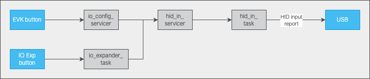
Fig. 60 HID button path with IO expander present#
Fig. 61 shows the updated path through which a HID output report translates into a GPO LED state change.
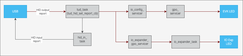
Fig. 61 HID LED path with IO expander present#
Note
The system design can be modified to support an I2C expander different from the PCAL6416A. Section Adding a different I2C Expander describes the steps required to do so.
HID Operation with expanded GPIO set#
With the I2C expander providing extra buttons and LEDs available to map to HID events, some more use cases are implemented as described below.
Handle Incoming Call#
Fig. 62 shows the device handling an incoming Teams call. The two scenarios shown are the user choosing to accept or reject the call by pressing the respective buttons on the device.
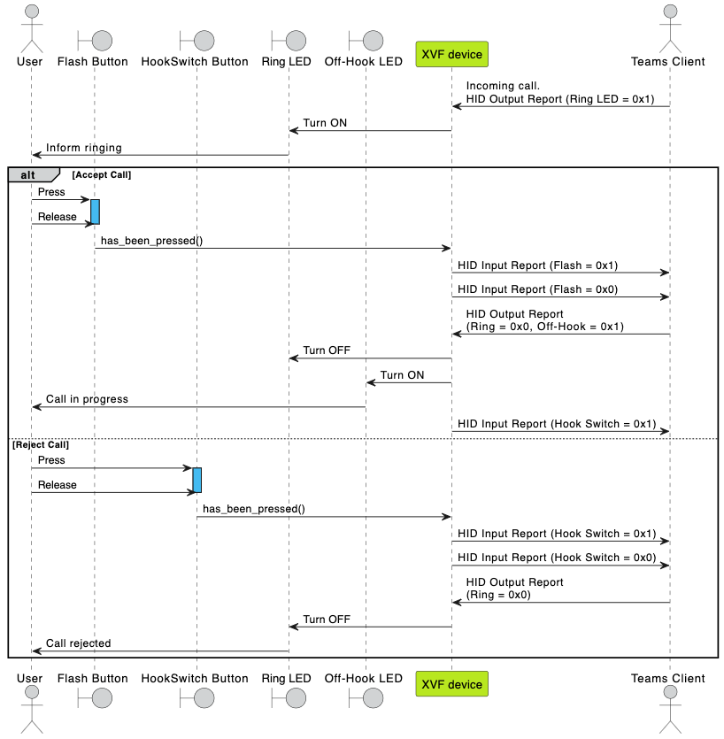
Fig. 62 Handle Incoming Call#
End Call#
Fig. 63 shows the user ending an ongoing Teams call by pressing a button on the device. This use case assumes an ongoing call as its precondition.
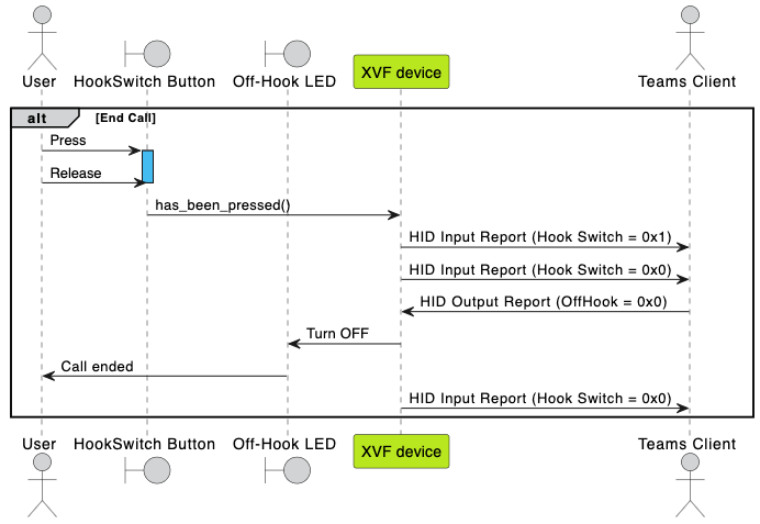
Fig. 63 End Call#
Hold/Unhold Call#
Fig. 64 shows the use case for placing an ongoing Teams call on hold, followed by bringing an on-hold call off hold. This use case assumes as ongoing call as its precondition.
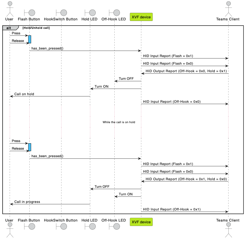
Fig. 64 Hold/Unhold Call#
Volume Increment/Decrement#
Fig. 65 shows the user adjusting the device volume by pressing the Volume up or down buttons on the device.
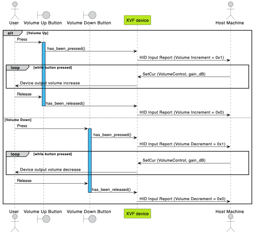
Fig. 65 Adjust Volume#
Note
Unlike the other use cases, the volume buttons work outside of a Teams call as well. Pressing the volume button on the device has the host send SetCur volume control commands on Endpoint 0 for controlling the USB output volume. The volumes buttons are Re-Trigger Control (RTC) type which means the host continues to send the SetCur commands as long as the button is pressed.